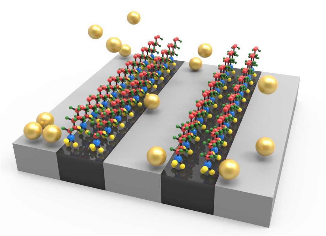
Despite this tremendous success, the paradigm described above is under stress. Were it not for the recent commercialization of EUV lithography, Moore’s Law would arguably have come to an end in 2019. Moreover, even though the microelectronics industry was pioneered in the United States, the U.S. risks losing its leadership position in the actual manufacturing of these critical devices since the most advanced patterning technologies have only been successfully applied to manufacturing abroad. Additionally, the path to future computing paradigms such as useful and ubiquitous quantum computing is predicated on achieving unprecedented patterning precision at large volumes.
It is evident that continued progress in microelectronics, as well as maintaining U.S. advanced manufacturing leadership, is predicated on future advancements in patterning methods and materials. Even future technologies that are arguably less dependent on two-dimensional scaling, such as quantum computing and spin-based systems, are, in fact, also patterning constrained because achieving their promise requires patterning precision well beyond the limitations of current methods and materials. Continued advancements in at-scale patterning methods to the realm of atomic scale precision is critical to realizing the potential of future generation memory and logic devices that will in turn enable transformative compute capabilities, while minimizing compute center carbon footprints.
Delivering on the technological impact described above will first require scientific breakthroughs in the fundamental understanding and deterministic control of materials at the atomic scale. Patterning in the context of advanced manufacturing of microelectronics relies on an extremely diverse and complicated set of materials and processes including: precision synthesis of functional materials; radiation sensitivity including ionization and fragmentation; low energy electron scattering and low energy electron attachment chemistry; control and confinement of these processes at the atomic scale; macromolecular effects and solvation of the modified material focusing in particular on the liquid/solid interface, pattern transfer via etch and/or selective deposition. Moreover, because these processes all need to occur in films nearing thicknesses in the single digit nm regime, interfacial issues including both macromolecular effects as well as low-energy electron cascade effects become critical.